Spin-resolved oscilloscope for charge and spin signals
Researchers at the Tokyo Institute of Technology and Nippon Telegraph and Telephone Corporation have developed a "spin-resolved oscilloscope." This device is a basic measuring instrument for plasmonics and spintronics, which are key technologies for future electronics applications. The coupling of light and electronic charges in plasmonics will pave the way for ultra-high-speed information processing, whereas spintronics will provide low-energy-consumption technology in a highly information-oriented society. The spin-resolved oscilloscope pioneers future "spin-plasmonics," where ultra-high-speed low-energy-consumption devices will be achieved.

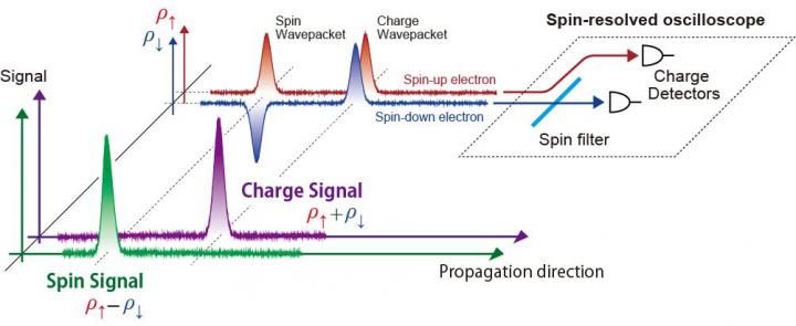
The spin-resolved oscilloscope is established by combining spintronic and plasmonic devices, i.e., a spin filter and time-resolved charge detectors.
Masayuki Hashisaka
An electron has charge and spin, and both the charge- and spin-density excitations in an electronic system can be utilized in information processing. The dynamics of charge-density waves has been investigated in plasmonics, and that of spin-density waves has been studied in the field of spintronics. However, less effort has been devoted to combining these two technologies and to developing the expected ultra-high-speed and low-energy-consumption devices. To date, a major obstacle preventing the promotion of this research field has been the lack of a measuring instrument that is sensitive to both charge and spin.
In their recent paper Dr. Masayuki Hashisaka at Tokyo Tech and colleagues reported a "spin-resolved oscilloscope" that enables measurement of the waveforms of both charge and spin signals in electronic devices. An oscilloscope is a basic measuring instrument used in electronics; however, conventional oscilloscopes do not facilitate both charge and spin measurement.
The "charge signal" is the total charge of the spin-up and -down electron densities. Further, the "spin signal" is the difference between the spin-up and -down electron densities. Both these signals traveling in a semiconductor device can be detected by the spin-resolved oscilloscope, which is composed of a spin filter and nanometer-scale time-resolved charge detectors. The spin filter separates the spin-up and -down electrons, while the time-resolved charge detector measures the waveforms of the charge-density waves. By combining these spintronic and plasmonic devices, the spin-resolved oscilloscope is established.
Using this spin-resolved oscilloscope, Hashisaka and colleagues demonstrated waveform measurements of charge- and spin-density wavepackets in a semiconductor device. They succeeded in observing the spin-charge-separation process in a one-dimensional (1D) electronic system composed of quantum Hall edge channels, which is a prototypical system for the investigation of 1D electron dynamics. This was the first experiment in which a single spin-charge-separation waveform measurement allowed estimation of all the relevant system parameters. Further, this observation manifests not only the usefulness of the spin-resolved oscilloscope, but also the possibility for developing novel plasmonic and spintronic devices based on 1D semiconductor materials.
The spin-resolved oscilloscope will promote investigations in both plasmonics and spintronics; for example, this device will aid studies of electron dynamics in various 1D systems. In addition, the spin-resolved oscilloscope will pave the way for future "spin-plasmonics," where ultra-high-speed and low-energy-consumption devices will be achieved.
Original publication
Other news from the department science

Get the analytics and lab tech industry in your inbox
By submitting this form you agree that LUMITOS AG will send you the newsletter(s) selected above by email. Your data will not be passed on to third parties. Your data will be stored and processed in accordance with our data protection regulations. LUMITOS may contact you by email for the purpose of advertising or market and opinion surveys. You can revoke your consent at any time without giving reasons to LUMITOS AG, Ernst-Augustin-Str. 2, 12489 Berlin, Germany or by e-mail at revoke@lumitos.com with effect for the future. In addition, each email contains a link to unsubscribe from the corresponding newsletter.
Most read news
More news from our other portals
Last viewed contents

A new animal model to understand metastasis in sarcomas
PerkinElmer Announces Global R&D Expansion in Singapore - New Center of Excellence Focused on Solutions for Environmental Health, Food Safety and Drug Discovery


