Smallest nanoantennas for high-speed data networks
More than 120 years after the discovery of the electromagnetic character of radio waves by Heinrich Hertz, wireless data transmission dominates information technology. Higher and higher radio frequencies are applied to transmit more data within shorter periods of time. Some years ago, scientists found that light waves might also be used for radio transmis-sion. So far, however, manufacture of the small antennas has required an enormous expenditure. KIT scientists have now succeeded for the first time in specifically and reproducibly manufacturing smallest optical nanoantennas from gold.
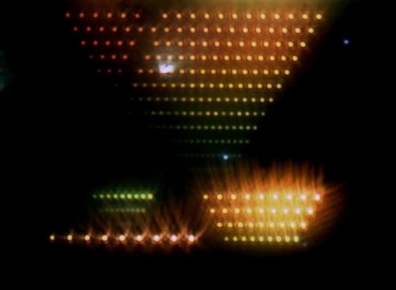
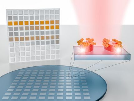
Pictured are nano dipole antennas under a microscope. The colors reflect the different transmission frequencies.
LTI
In 1887, Heinrich Hertz discovered the electromagnetic waves at the former Technical College of Karlsruhe, the predecessor of Univer-sität Karlsruhe (TH). Specific and directed generation of electro-magnetic radiation allows for the transmission of information from a place A to a remote location B. The key component in this transmis-sion is a dipole antenna on the transmission side and on the recep-tion side. Today, this technology is applied in many areas of every-day life, for instance, in mobile radio communication or satellite re-ception of broadcasting programs. Communication between the transmitter and receiver reaches highest efficiency, if the total length of the dipole antennas corresponds to about half of the wavelength of the electromagnetic wave.
Radio transmission by high-frequency electromagnetic light waves in the frequency range of several 100,000 gigahertz (500,000 GHz correspond to yellow light of 600 nm wavelength) requires minute antennas that are not longer than half the wavelength of light, i.e. 350 nm at the maximum (1 nm = 1 millionth of a millimeter). Con-trolled manufacture of such optical transmission antennas on the nanoscale so far has been very challenging worldwide, because such small structures cannot be produced easily by optical exposure methods for physical reasons, i.e. due to the wave character of the light. To reach the precision required for the manufacture of gold antennas that are smaller than 100 nm, the scientists working in the "Nanoscale Science" DFG-Heisenberg Group at the KIT Light Tech-nology Institute (LTI) used an electron beam process, the so-called electron beam lithography. The results were published recently in the Nanotechnology journal.
These gold antennas act physically like radio antennas. However, the latter are 10 million times as large, they have a length of about 1 m. Hence, the frequency received by nanoantennas is 1 million times higher than radio frequency, i.e. several 100,000 GHz rather than 100 MHz.
These nanoantennas shall transmit information at extremely high data rates, because the high frequency of the waves allows for an extremely rapid modulation of the signal. For the future of wireless data transmission, this means acceleration by a factor of 10,000 at reduced energy consumption. Hence, nanoantennas are considered a major basis of new optical high-speed data networks. The positive side-effect: Light in the range of 1000 to 400 nm is not hazardous for man, animals, and plants.
In the future, nanoantennas from Karlsruhe may not only be used for information transmission, but also as tools for optical microscopy: "With the help of these small nano light emitters, we can study indi-vidual biomolecules, which has not been established so far", says Dr. Hans-Jürgen Eisler, who heads the DFG Heisenberg group at the Light Technology Institute. Moreover, the nanoantennas may serve as tools to characterize nanostructures from semiconductors, sensor structures, and integrated circuits. The reason is the efficient capture of light by nanoantennas. Thereafter, they are turned into light emitters and emit light quantums (photons).
The LTI scientists are presently also working on the specific and efficient capture of visible light by means of these antennas and on focusing this light on a few 10 nm, the objective being e.g. the opti-mization of photovoltaic modules.
Original publication: Nanotechnology 20 (2009) 425203
Most read news
Topics
Organizations
Other news from the department science

Get the analytics and lab tech industry in your inbox
By submitting this form you agree that LUMITOS AG will send you the newsletter(s) selected above by email. Your data will not be passed on to third parties. Your data will be stored and processed in accordance with our data protection regulations. LUMITOS may contact you by email for the purpose of advertising or market and opinion surveys. You can revoke your consent at any time without giving reasons to LUMITOS AG, Ernst-Augustin-Str. 2, 12489 Berlin, Germany or by e-mail at revoke@lumitos.com with effect for the future. In addition, each email contains a link to unsubscribe from the corresponding newsletter.
