World's smallest universal material testing system
The design, development and manufacturing of revolutionary products such as the automobile, airplane and computer owe a great deal of their success to the large-scale material testing systems (MTS) that have provided engineers and designers with a fundamental understanding of the mechanical behavior of various materials and structures.
In the world of nanotechnology, however, where the mechanical characterization of materials and structures takes place on the scale of atoms and molecules, the existing material testing systems are useless. The development of a universal nanoscale material testing system (n-MTS), which could fit in existing electron microscopes and possess the resolution and accuracy needed to mechanically test nanoscale objects, has been a major challenge within the scientific community.
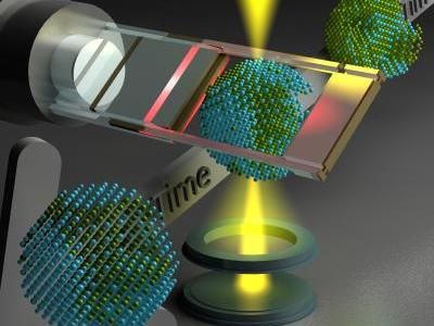
Now researchers at Northwestern University have designed and built the first complete micromachine that makes possible the investigation of nanomechanics phenomena in real time. The findings are published online by the Proceedings of the National Academy of Sciences (PNAS). The machine, which can fit in tiny spaces as required by in situ transmission electron microscopy (TEM), successfully characterized the mechanical properties of nanowires and carbon nanotubes.
The n-MTS developed by Horacio D. Espinosa, professor of mechanical engineering, and his colleagues consists of an actuator and a load sensor fabricated by means of micro technology. The load sensor is based on differential capacitive sensing, which provides a load resolution of about 10 nano Newtons. This is the first nanoscale material testing system that provides continuous observation of specimen deformation and failure with sub-nanometer resolution while simultaneously measuring electronically the applied forces with nano-Newton resolution. The integration of electro-mechanical and thermo-mechanical components at the micro scale made the achievement possible.
One of the challenges overcome by the University researchers was the integration of micro-electro-mechanical systems (MEMS) and circuits for measurement of electronic signals. They solved this problem by using a double-chip architecture consisting of a MEMS chip and a microelectronic sensing chip. Another challenge overcome by the team was the mounting of individual nanostructures on the testing device. Using a nanomanipulator inside a dual-beam scanning electron microscope and focused ion beam apparatus the researchers picked up nanostructures, cut them to the desired length and nanowelded the structures onto the n-MTS using electron-beam-induced deposition of platinum.
As reported in the PNAS paper, the system capabilities were demonstrated by in situ electron microscopy testing of free-standing polysilicon films, metallic nanowires and carbon nanotubes (CNTs). Espinosa's team achieved the first real-time instrumented in situ transmission electron microscopy observation of CNTs failure under tensile loading.
Other news from the department science