Nanostructures stabilise lasers
Empa researchers use electron beams for chemical reactions
Electron microscopes use focussed electron beams to make extremely small objects visible. By combining the instrument with a gas-injection system material samples can be manipulated and surface structures measuring only nanometres across can be “written”. Empa researchers, together with scientists from EPFL, used this method to improve lasers.
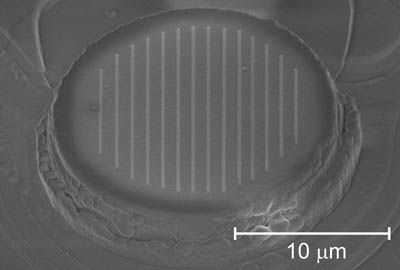
The result is a nanostructure – for example a polarisation grating on a VCSEL (vertical cavity surface emitting laser). These are semiconductor lasers frequently used in optical data transmission.
Empa
The principle of the local deposition process which is induced with a focussed electron beam (in short, FEBIP): molecules from a gas-injection system are deposited on the sample surface in a reversible manner. The focussed electron beam dissociates adsorbed gas molecules. The resulting non-volatile compounds remain permanently on the sample.
The vertical cavity surface emitting laser (VCSEL) is a semiconductor laser which is often used in data transmission for short-distance links like Gigabit Ethernet. These lasers are very popular in telecommunications because they consume little energy and can be simply fabricated in volumes of many tens of thousands on a single wafer. However, these VCSELs can exhibit one weakness: Because of the cylindrical structure in which the lasers are built up on the wafer, the polarisation of the emitted light can sometimes change during operation. Polarisation is a property of certain waves, such as light waves, and it describes the direction of oscillation. A stable polarisation is necessary in order to reduce transmission errors and to use VCSELs in future silicon photonics.
The team led by Empa researcher Ivo Utke, together with scientists from the Laboratory of Physics of Nanostructures at EPFL, could provide assistance by using a method called FEBIP (focussed electron beam induced processing). “We’ve written flat grating structures on the VCSELs with an electron beam,” says Utke in describing their solution, “and the gratings were effective in stabilising the polarisation.”
Small, minimally invasive, direct
FEBIP is suitable for prototyping nanocomponents, in order to solve specific questions and problems in applied nanoelectronics, nanophotonics and nanobiology. Suitable gas molecules are injected close to a sample which is already in the microscope’s vacuum chamber. These adsorb on the sample in a reversible manner. The focussed electron beam, which normally serves to make objects visible, now instead induces chemical reactions of the adsorbed gas molecules, but only at the spot where the beam strikes the surface. The resulting non-volatile molecular fragments then remain permanently on the sample while the volatile fragments are removed by the vacuum system. “With the help of a precisely positioned electron beam, it’s possible to remove or apply surface structures with nanometre precision and in virtually any desired three-dimensional shapes,” explains Utke. “FEBIP could soon become a true nanofabrication platform for rapid prototyping of nanostructures in a minimally invasive way, without necessitating the large investment of a clean room.”
Original publication

Other news from the department science